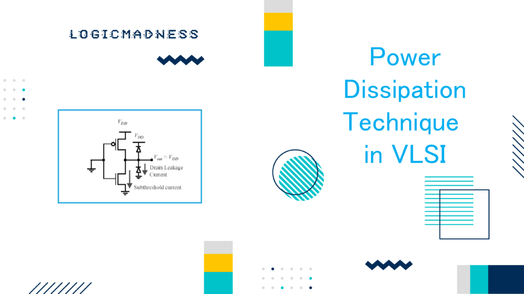
Retention Cells in VLSI are specialized sequential circuits designed to maintain their internal state even when the main power supply is turned off. They have the ability to restore this state once power is restored. One common type of retention cell is the Master/Slave Alive retention cell, which includes a standard flip-flop and a slave latch. The slave latch retains data during power outages, powered by an ‘Always ON’ (AON) supply. This latch employs high-threshold transistors to minimize leakage power. A control signal, known as the ‘SLEEP’ signal, manages the retention operations of the cell.
Why Do We Need Retention Cells in VLSI?
In many situations, it’s essential to retain the states of control flip-flops during power-gated (PG) mode. Without Retention Cells in VLSI, the output of PG cells could go to an unknown state (‘X’). If power is restored, this could lead to a metastable state in the logic.
For example, consider a finite state machine (FSM) operating in a power-gated domain while receiving input from an always-on domain. If the FSM is in state S2 when it enters power-gated mode, it will lose its state information once power is cut. When power is restored, the FSM will receive a known input but be in an unknown state, necessitating a reset to its default state, S0. This reset process can slow down the system, highlighting the need for retention cells, which can store the state even in power-gated mode.
State Transition Diagram of a Simple FSM

Regular Positive Edge-Triggered D Flip-Flop
Before diving deeper into retention cells, let’s review the regular D flip-flop. This flip-flop consists of two latches that activate when the enable signal is high.
Positive Edge-Triggered D Flip-Flop Timing Diagram

Timing Diagram of Internal Signals

Retention Cells in VLSI: Master/Slave Alive Retention Flop
In a Master/Slave alive retention flop, the slave latch connects to a separate, always-on power rail. When the cell enters power-gated mode, the SLEEP signal is asserted, cutting off VDD power. While the master latch becomes inactive, the slave latch continues to store data. To avoid data corruption, the SLEEP signal keeps the enable pin of the slave latch low.


Timing Diagram for Retention Flop

Timing Issues in Master/Slave Retention Flop
Challenges with Retention Cells in VLSI
- Leakage Power: High-threshold transistors reduce leakage power, but they can slow down performance compared to low-threshold transistors.
- Clock Dependency: The master/slave retention cell can only retrieve its state when the clock (CLK) is low.
- Area Constraints: Other types of retention cells may mitigate these issues but typically require more area.
- Power Supply Complexity: All retention cells need two power supplies: a switchable power supply that turns off in PG mode and an AON supply, complicating power routing.
Retention Cells in VLSI Control Strategies
Set Retention
This command specifies which elements in the power-gated domain should retain their values when power is off.
set_retention retention_name
   – domain domain_name
   – retention_power_net net_name
   – retention_ground_net net_name
   – elements list
Arguments of Retention Cell
| Argument | Description |
| retention_name | Name for the retention strategy. |
| – domain domain_name | The domain where the strategy applies. |
| – retention_power_net net_name | Supply net for retention logic. |
| – retention_ground_net net_name | Ground net for retention logic. |
| – elements list | List of registers affected by this strategy. |
Set Retention Control
This command defines the control signals for a specified retention strategy.
Syntax:
set_retention_control retention_name
   – domain domain_name
   – save_signal signal < high | low >
   – restore_signal signal < high | low >
Arguments of retention control
| Argument | Description |
| retention_name | Corresponding retention strategy name. |
| – domain domain_name | The domain where the strategy is applied. |
| – save_signal signal < high | low > |
| – restore_signal signal < high | low > |
Note: Typically, the save and restore signals are the same but have different active levels.
Types of Retention Cells in VLSI
Retention cells can be classified based on how values are stored and retrieved:
- Balloon-Style Retention: This style holds the retained value in an additional latch (balloon latch) that is not part of the functional data path.
- Master/Slave-Alive Retention: This style retains the value in the master or slave latch, placing it in the functional data path.
Comparison of Retention Cells in VLSI Types
| Type | Description | Control Signals |
| Balloon-Style | Value held in an additional balloon latch. | Separate for save/restore |
| Master/Slave-Alive | Value retained in master or slave latch. | Usually none; retention state is automatic |
Additional Types of Retention Cells in VLSI
Dual-Pin Retention
- Description: Utilizes two separate control signals for save and restore operations. The save operation can be level-sensitive or edge-sensitive.
Single-Pin Retention
- Description: Uses a single control signal for both save and restore operations, but operates on opposite signal levels.
Zero-Pin Retention
- Description: No control signals are present. Save operations occur when the power domain transitions from normal to corrupt, and restore operations occur when it transitions back.
Summary of Retention Cells in VLSI
Retention cells are crucial components in modern ASIC design, particularly in systems with multiple power domains. In power-aware RTL design, retention cells integrate with UPF (Unified Power Format) and CPF (Common Power Format). The two main types of retention cells are Balloon Type and Master-Slave Type.
Power Management Methods
Modern chips utilize various power management techniques, including:
- Multiple Threshold Voltages (Multi-Vt)
- Multiple VDDs for different domains
- Power Gating to manage power between blocks
- Clock Gating to optimize clock cells
- Dynamic Voltage Scaling (DVS) and Dynamic Frequency Scaling (DFS)
Standard cells like retention flops, isolation cells, power switch cells, and level shifter cells contribute significantly to effective power management.
Conclusion
Retention cells play a vital role in preserving the state of circuits during power down periods, enabling faster recovery and improved efficiency in integrated circuits. They are essential for chips that operate with multiple power domains and support power-gating techniques effectively.