FPGA synthesis is the process of converting a high-level design description, typically written at the Register Transfer Level (RTL), into a gate-level representation. The goal of synthesis is to transform the RTL code into a form that can be mapped onto an FPGA (Field-Programmable Gate Array) chip and fabricated.
Synthesis Process = Translation + Logic Optimization + Mapping
Why Do We Need FPGA Synthesis?
FPGA synthesis is a crucial step in chip design because it allows engineers to understand how their design will look and behave after manufacturing. This process enables us to:
- Convert RTL code into basic logic gates.
- Map those gates to specific technology-dependent gates from a library.
- Optimize the design while adhering to the design constraints (such as area, power, and timing).
The main goals of FPGA synthesis are:
- Create a gate-level netlist.
- Insert clock gates.
- Perform logic optimization.
- Maintain logic equivalence between the RTL code and the synthesized netlist.
- Add Design for Test (DFT) logic to aid in testing.
FPGA Synthesis Flow
The FPGA synthesis flow involves several stages, each designed to achieve a specific goal. Let’s break down these stages.
1. Inputs Required for FPGA Synthesis
To begin synthesis, the following inputs are required:
- High-Level Description (RTL Code): Written in hardware description languages (HDL) like Verilog or VHDL, this code defines the behavior of the digital circuit.
- Design Constraints: These include timing, area, power, and other performance requirements that influence how the design is implemented.
2. Elaboration Stage
In this stage, the high-level description (RTL code) is parsed and analyzed. The design is divided into modules and submodules, establishing a hierarchy. Basic checks are performed to verify that the design follows the syntax and semantic rules of the chosen HDL.
Design Constraints (XDC File): This file contains important design information such as timing constraints, wire load models, and other parameters like DRVs (Design Rules Violations). DRVs include:
- Hard Constraints (Max Transition, Max Capacitance): These must be met and cannot be violated.
- Soft Constraints (Max Fanout, Max Length): These can be ignored if violated.
3. Generic Stage (Logical Synthesis)
At this stage, the high-level design is converted into a generic gate-level representation. This involves turning behavioral descriptions into structural ones, using basic logic gates like AND, OR, NAND, and NOR. The goal is to preserve functionality while optimizing for:
- Area
- Power consumption
- Timing
4. Mapping and Optimization Stages
Once the design is in a generic gate-level format, the next step is to map the design to specific gates in the target technology library.
- Technology Mapping: The generic gate-level representation is translated into the technology-dependent gates available in the standard cell library.
- Logical Optimization: This includes techniques like Boolean logic simplification, constant propagation, and common subexpression elimination to improve performance, reduce power, and save space.
- Timing Optimization: Ensures the design meets timing requirements by adjusting delays or adding buffers.
- Area Optimization: Aims to reduce the physical space the design occupies on the FPGA.
Ensuring Accuracy with Verification and Testing
After synthesis, it is critical to verify and test the synthesized design. Verification ensures that the design behaves as expected and matches the original RTL code.
- Testbench Development: A testbench is created to supply inputs to the synthesized design. This helps in checking how the design behaves under various scenarios, including edge cases.
- Simulation and Formal Verification: Various methods like simulation and formal verification are used to validate the design’s functionality.
Iterative Process
During verification, designers may loop back to the synthesis process to fix any issues or discrepancies that arise. This iterative approach ensures a final design free of errors and ready for implementation.
Example: Verifying a Synthesized Design
Imagine you’ve written an RTL description for a complex digital circuit. After synthesis, you want to make sure the physical version of your circuit matches the original design. You use a testbench to simulate different conditions and run formal tests. If any issues are found, you refine the design and repeat the process.
Important FPGA Synthesis Reports
Several reports are generated during the FPGA synthesis process. These reports provide valuable insights into the design’s performance, resource utilization, and potential issues.
| Report | Description |
|---|---|
| Synthesis Report | Provides an overview of the synthesis process, detailing logic optimizations, errors, and design hierarchy. |
| Timing Summary Report | Analyzes timing paths, critical paths, and timing slack to ensure the design meets the required performance. |
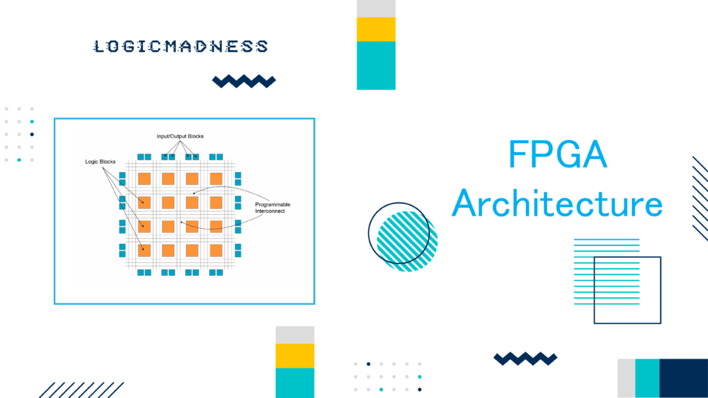
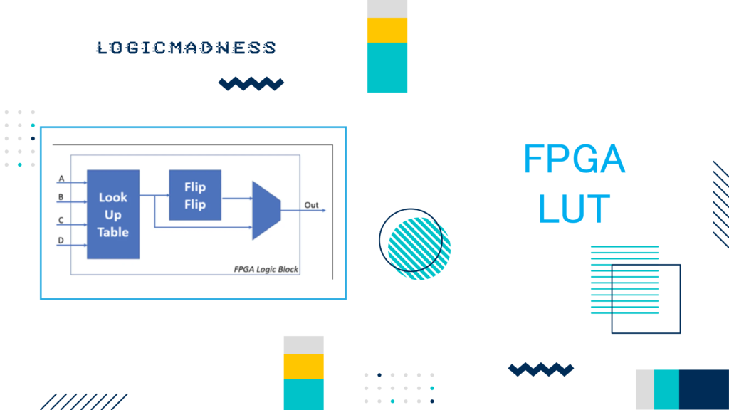
| Utilization Report | Breaks down FPGA resource usage (e.g., LUTs, flip-flops, I/O pins) to ensure efficient use of FPGA resources. |
| Area Constraints Report | Compares actual area usage with specified area constraints, helping to identify over or underutilization. |
| Power Report | Estimates power consumption based on design resource usage and provides insights into power optimization. |
| DRC Report | Checks for design rule violations to ensure compliance with FPGA architecture standards. |
Final Steps: Moving to Implementation
Once the synthesis, optimization, and verification processes are complete, the design is ready for the next stage: Implementation. Congratulations on achieving this important milestone!
Example Code: FPGA Synthesis in Verilog
Here’s an example of a simple FPGA design written in Verilog, with variable names changed for clarity:
module simple_adder(
    input wire a,
    input wire b,
    input wire c_in,
    output wire sum,
    output wire carry_out
);

    wire sum1, carry1, carry2;

    // First half adder
    assign sum1 = a ^ b;
    assign carry1 = a & b;

    // Second half adder
    assign sum = sum1 ^ c_in;
    assign carry2 = sum1 & c_in;

    // Final carry-out
    assign carry_out = carry1 | carry2;

endmodule
Explanation:
- sum1 and carry1 are intermediate signals used to compute the sum and carry for the first half adder.
- carry2 is the carry from the second half adder.
- The final carry-out is computed by OR-ing the two carry signals.
In this example, variable names have been changed for better clarity, and the code structure is kept simple to illustrate the synthesis process.